Best Pcb DesignTraining Institute in Mohali - Chandigarh - Punjab
PCBA2Z is an initiative by group of Qualified Senior Design Engineers with a very good Practical Experience in the field who don’t just design but actually train engineers. PCBA2Z is a plethora of events where budding minds will learn through hands on development of live projects ranging from technical workshops, seminars, guest lectures and competitions.
Schematic Capture
- New Project Creation
- Single and multiple sheets designs
- Selecting components from Libraries
- Making New Components
- Bill of Material Creation
- Net-list creation
- Introduction to Thru hole and SMT components
- Creation of PCB Footprints both in mm and mils
PCB Layout
- Import Net list in to Pcb Package
- Selection of Pcb footprints from Library
- Making New Components – Pcb footprints
- Selection of Layers
- Selection and Placement of Components
- Routing – tracks
- Single Layer and Double Layer PCB Designs
- Inter communication tools
Students first step towards PCB Layout Design
We also conduct workshops deals with designing of printed circuit board.
In workshop students came to know about Functions of PCB’s, Types of Pcb’s, Classifications of PCB’s, Base material in addition to design Single and Double Layer PCB’s
This workshop will not only provided them theoretical knowledge but will also provide them with hands-on practical learning experience- a unique initiative by PCBA2Z Solutions.
Workshop Outline:
This workshop basically deals with designing of printed circuit board. After the workshop students come to know
About Functions of PCB’s, Types of Pcb’s, Classifications of PCB’s, Base material in addition to Design Single and Double Layer PCB’s using CAD.
This workshop will not only provided them theoretical knowledge but will also provide them with hands-on practical
Learning experience – a unique initiative by PCBA2Z Solutions
Introduction to PCB’s
- Classification of PCB
- Base material
- Parts of PCB
- PCB Manufacturing Technology
- Steps in PCB Fabrication
Schematic Capture
PCB Design Process
- New Project Creation
- Single and multiple sheets designs
- Connectivity of all sheets
- Selecting components from Libraries
- Making New Components
- Check DRC
- Bill of Material Creation
- Net-list creation
- Introduction to thru hole and SMT components
- Study of datasheets of Electronics components
- Creation of PCB Footprints both in mm and mils
PCB Layout
- Import Net list in to Pcb Package
- Selection of PCB footprints from Library
- Making New Components – PCB footprints
- Selection of Layers
- Selection and Placement of Components
- Routing – tracks
- Single Layer and Double Layer PCB Designs
- Inter communication tools – cross probing
Gerber Data Generation
Penalization – Edit Gerber
- We are flexible to incorporate any changes as per Institute’s requirement.
- We look forward for a long term association with you.
- Job Oriented Certificate Course on Printed Circuit Board Design
Eligibility:
- 10+2 / I.T.I / Diploma / B.E. / B. Tech / B.Sc. / M.Sc. / M.E. / M. Tech in Electronics / Telecommunication / Instrumentation / Electrical / Mechatronics / Electronics Technicians
- Other Students with little knowledge of electronics can also join.
Outcome:
On completion of the Course…
Students can explore different aspect of Printed Circuit Board Design and fabrication.
- Students can learn various types of PCB’s Schematic Design. Rules for Schematic Entry, Component Layout methods
- Placement Rules, Routing Techniques for Single Sided Board
- Post Processing of design and Fabrication documents.
- After completing this course students can design and fabricate their own PCB for their Project and can also work in PCB Designing and Fabrication area.
- Why PCB Design & Manufacturing?
- The Printed Circuit Board (PCB) is very important in all electronic gadgets, which are used either for domestic use, or for industrial purpose.
- PCB design services are used to design the electronic circuits.
- PCBs are the core component in almost all the electronic gadgets including the cell phones and the computers and laptops.
- With the increase in demand, the number of PCB services is on the rise.
- An effective PCB design can help in reducing the possibilities of errors and the chances of short circuit.
- A creative PCB designer has great chances to explore the field.
Career Prospects:
- It Pays Handsomely
- You Can Choose from a Variety of Job Roles
- PCB Design Is Growing Rapidly
- It is challenging
- Big Organizations are looking for you
- It Has an Excellent Online Community
- It Is Easy to learn
Expected Remuneration:
- If you are a fresher working in this field then you may get a starting salary of 3.4 Lac / Year to 5.3 Lac / Year.
Training Fee:
- INR 7500/- for Single layer PCB design (Basic Course) Duration: 30 Days
- INR 15,000/- For Double Layer Pcb design training (Advance Course) Duration: 45 Days
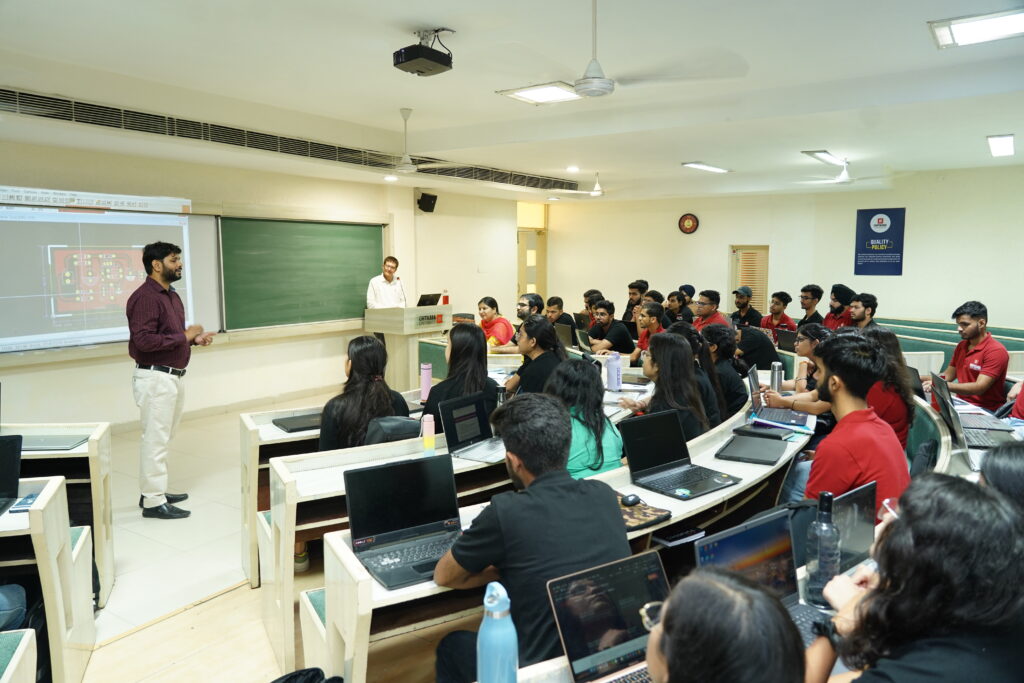
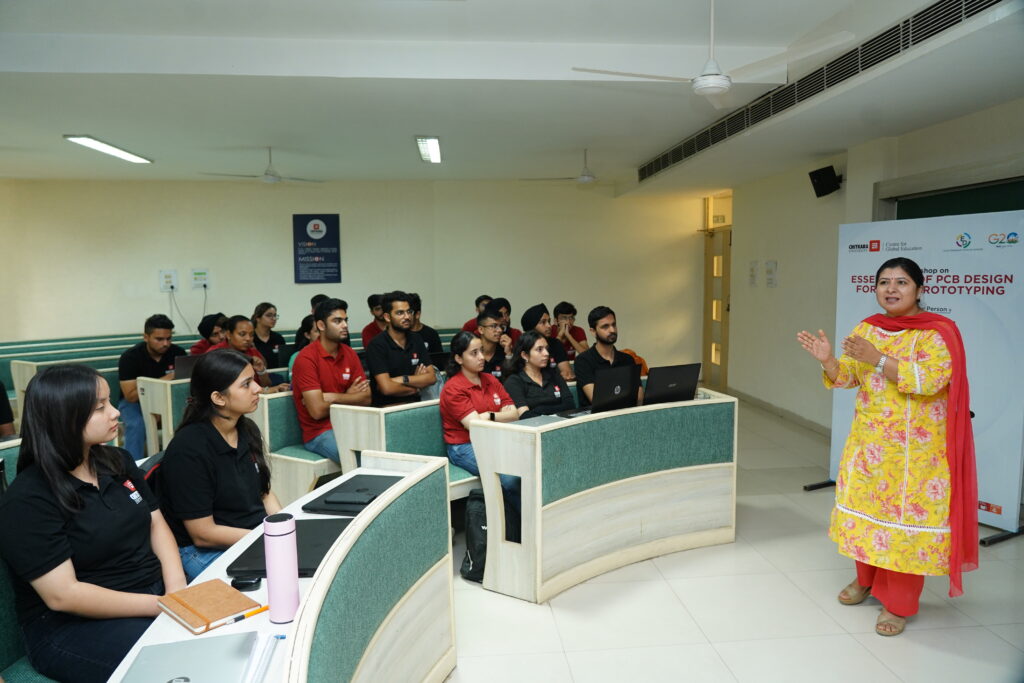
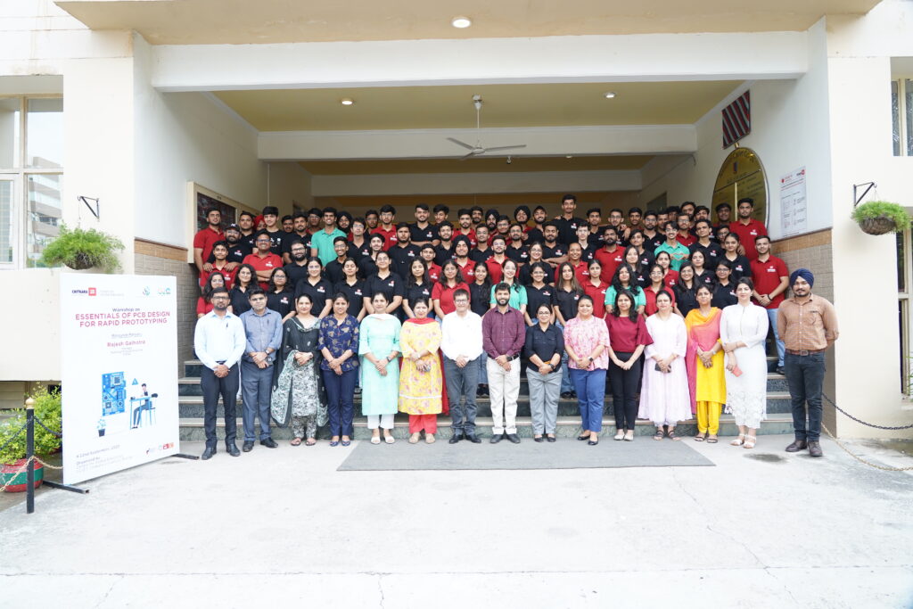
Workshop at Chitkara University
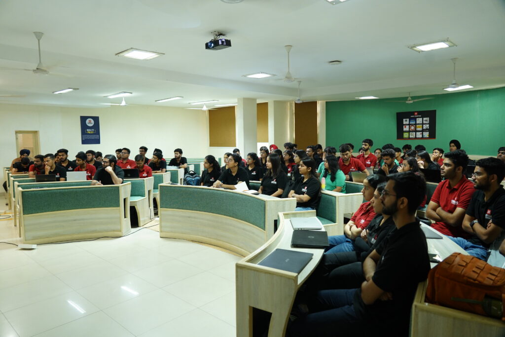
Workshop at RIMT University

Student Success Stories
What Our Graduates Are Saying About Their Journey